This site uses cookies to offer you a better browsing experience. By continuing to navigate through this site or by clicking Approve, you consent to the use of cookies on your device as described in our privacy notice.
Scanning Electron Microscope (SEM)

Scanning Electron Microscope (SEM)

Powerful surface imaging and analysis—made smarter.

At BCL, we bring you the latest generation of JEOL Scanning Electron Microscopes (SEM)—engineered for unmatched surface observation, analysis, and precision. Whether you're in R&D, quality testing, or materials science, JEOL SEMs deliver the versatility and performance today’s labs demand.

From compact benchtop models for general use to high-end Field Emission SEMs (FE-SEM) for ultra-fine resolution, JEOL offers scalable solutions for every application. And with in-house developed Energy-Dispersive X-ray Spectrometers (EDS), elemental analysis is seamlessly integrated into your workflow.


Enquiry

Schottky Field Emission Scanning Electron Microscope

Where cutting-edge clarity meets intelligent automation.

The JSM-IT810 is engineered for innovators who demand uncompromising image resolution and intelligent functionality in one seamless package. This advanced Schottky Field Emission SEM merges high-definition surface imaging with next-gen automation—streamlining your entire workflow from visual capture to elemental insight.

With a design philosophy rooted in precision, adaptability, and simplicity, the IT810 transforms complex analysis into a frictionless, user-friendly experience—whether you're conducting in-depth materials research or fast-paced quality control.

Signature Features:

  • Neo Action: Intelligent Automation, Zero Programming
    Automate your SEM and EDS operations with just a few clicks—simply choose the area and conditions, and the system takes over from there.
  • Self-Calibrating Intelligence (Optional)
    Keep your system finely tuned with automated beam alignment, magnification checks, and energy calibration—all powered by a dedicated reference sample.
  • Dynamic 3D Surface Mapping
    Experience real-time topographic depth with our specialized BSE detector, creating live 3D reconstructions ideal for EBSD workflows and surface morphology studies.
  • Fluid SEM–EDS Integration
    Break down analytical silos—plan, observe, and analyze (point, area, map, or line) all from a unified interface without toggling between platforms.

Purpose-Built For:

  • Advanced Materials & Nanotech Labs needing ultra-fine spatial resolution and rich surface profiling at the micro and nano scale.
  • Product Reliability & Failure Analysis Teams seeking accurate, high-throughput elemental verification—without the operational complexity.
  • Collaborative, Multi-User Facilities where automated workflows reduce training time and ensure repeatable, reliable imaging across users.
  • High-Volume R&D Environments where speed, automation, and precision must work in perfect harmony.

High-Resolution SEM with Next-Gen Imaging

The JSM-IT710HR is a high-performance SEM that makes high-resolution imaging accessible to everyone. It features JEOL’s fourth-generation high-resolution platform, combining intuitive controls, advanced automation, and powerful imaging capabilities in a single tool.

Highlights:

  • Superior Image Quality: See SEM and optical images side-by-side for effortless navigation and targeting.
  • Live 3D Imaging: Instantly visualize surface contours with a 4-direction BSE detector that constructs real-time 3D images.
  • Next-Level Automation: Automatic beam alignment, astigmatism correction, and focus adjustment—no manual tuning needed.
  • New LHSE Detector (Optional): Switch between topographic and light-emission imaging modes for more versatile low-vacuum observation.
  • Zeromag Navigation: Link SEM and optical views to simplify your workflow and speed up analysis.

Built for:

  • Advanced Materials Science & Nanotechnology Research that demands ultra-high resolution and real-time topographic imaging to study fine structures and complex surfaces.
  • High-Throughput Industrial Labs where fast, automated data acquisition and analysis are essential to meet tight production or development timelines.
  • Academic and Government Research Institutions that need powerful imaging performance in a user-friendly platform suitable for students, researchers, and specialists alike.
  • Electron Microscopy Core Facilities that support a broad range of applications and require reliable, high-performance SEMs with easy navigation and automated operation.

Compact Scanning Electron Microscope for Efficient Everyday Use

Smart, streamlined, and ready to perform.

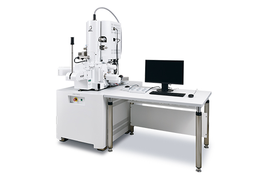
The JSM-IT210 is JEOL’s most compact stationary SEM—designed for labs that need high-performance imaging and elemental analysis in a user-friendly, space-saving system. Built with a motorized 5-axis stage and guided workflows, the JSM-IT210 ensures safe, accurate, and fully automated observations, even for first-time users.

Whether you’re dealing with delicate, heat-sensitive specimens or need fast EDS analysis across multiple sites, this SEM handles it all—with minimal supervision and maximum productivity.

Highlights

  • Specimen Exchange Navi
    Step-by-step guidance from sample loading to automatic observation—safe and effortless.
  • Zeromag Navigation
    Seamless transition from optical to SEM image with linked views for easy targeting.
  • Live EDS Analysis
    View elemental composition in real-time during observation—ideal for fast decisions.
  • Simple SEM Automation
    Automatically capture images across multiple areas, settings, and magnifications.
  • Standard 60 mm² EDS Detector
    Fast, high-quality elemental mapping with reduced beam damage—perfect for delicate samples.
  • Precision Motorized Stage
    Accurate, 5-axis movement ensures smooth repositioning and repeatable analysis.

Ideal For

  • Educational Institutions & Entry-Level Labs where compact size, ease of use, and guided workflows make SEM accessible for students and technicians.
  • QA/QC and Production Support Teams needing fast, repeatable observations and real-time EDS analysis without complex setup.
  • Facilities Handling Heat-Sensitive or Fragile Specimens, such as polymers, coatings, and biological materials, thanks to its gentle imaging capabilities.

Multi-Sample Environments that benefit from unattended operation and batch imaging, boosting lab efficiency and freeing up operator time.

Smart Scanning Electron Microscope for Efficient Everyday Imaging

Do more, faster—with automated ease.

The JSM-IT510 is the perfect balance between performance, usability, and automation. Built for both research and industrial environments, this SEM streamlines routine observations and analysis, making your workflow smoother and more efficient. With features like Simple SEM, Specimen Exchange Navi, and Live EDS Analysis, even repetitive tasks become effortless.

Whether you’re analyzing metals, polymers, biological specimens, or electronic components, the IT510 delivers fast, reliable results with minimal manual input.

Highlights

  • Simple SEM Automation
    Let the system handle routine operations—just select your target field, and it does the rest.
  • Specimen Exchange Navi
    Guided sample setup and automatic observation after vacuuming—safe, fast, and hands-free.
  • Zeromag Navigation
    Smooth transition from optical to SEM imaging with full-screen navigation and linked views.
  • Live EDS Analysis
    Instantly see spectra or elemental maps during observation—ideal for quick identification.
  • Optional Live 3D & LHSED
    Enhance topography with real-time 3D imaging or view combined photon/electron signals for richer surface detail.

Ideal For

  • Quality Assurance & Process Control teams needing repeatable, fast SEM imaging in manufacturing or production settings.
  • R&D Laboratories looking for a reliable SEM that simplifies workflows and supports multi-user environments.
  • Educational Institutions where user-friendly interfaces and automated features reduce the learning curve.
  • Material & Component Inspection across electronics, automotive, polymers, and more—with fast EDS mapping and 3D visualization options.

Next-Gen Benchtop SEM for Effortless Imaging & Analysis

Big performance. Small footprint. Seamlessly smart.

The JCM-7000 NeoScope™ redefines benchtop SEMs by combining high-resolution imaging, real-time elemental analysis, and unmatched user simplicity—all in a remarkably compact design. Built for fast-paced environments, this smart system brings advanced surface analysis to your desktop, making it an essential tool for today’s quality labs, production lines, and research teams.

With innovative functions like Zeromag, Live EDS, and Low-Vacuum observation, the JCM-7000 delivers fast, accurate insights across a broad spectrum of applications—from industrial materials to food safety.

Key Advantages at a Glance:

  • Zeromag Navigation
    Glide effortlessly from optical to SEM mode with pinpoint precision—no guesswork, just clarity.
  • Live Elemental Mapping
    Instantly visualize composition with embedded Live Analysis—see the spectrum and element maps as you scan.
  • Real-Time 3D Surface Reconstruction (Optional)
    Visualize textures and surface morphology in vivid detail with dynamic, live 3D imaging.
  • Low-Vacuum Versatility
    Examine non-conductive or delicate samples like polymers, powders, and organic matter—no coating or pre-treatment required.
  • Compact & Lab-Ready
    Small enough to sit beside your optical scope; powerful enough to elevate your entire inspection process.

Perfectly Suited For:

  • On-the-Spot QA/Inspection in electronics, automotive, pharma, and packaging—detect defects, contamination, or material variation instantly.
  • In-House Failure Analysis & Troubleshooting—eliminate wait times by handling surface diagnostics directly on-site.
  • Cross-Disciplinary Research Labs needing a fast, intuitive SEM for multi-material analysis without operator complexity.
  • Teaching & Skill Development Centers, where simplified controls and instant results support immersive, hands-on learning.

Contact Us at +9714 2152799

We can help you with a solution tailor to your specific need.