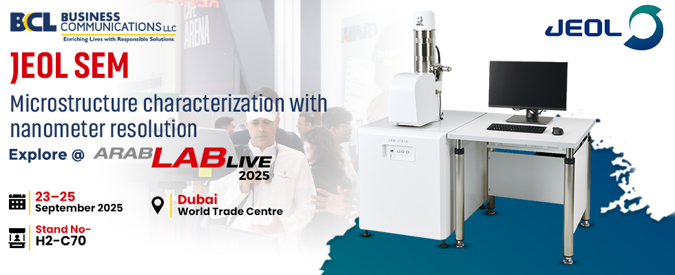
Get Close to the Micro World: JEOL SEM Live at BCL’s ArabLab Exhibition
Every surface, structure, and material carries secrets invisible to the naked eye. Whether it is the intricate texture of a butterfly wing, the grain structure of steel, or the nanoscale architecture of semiconductor materials, the details lie hidden in dimensions far smaller than a strand of human hair.
For decades, scientists have relied on the electron microscope to uncover this unseen world. At ArabLab 2025, visitors will have the chance to experience this power up close, as BCL showcases the advanced JEOL Scanning Electron Microscope (SEM).
How SEM Transforms Research
Optical microscopes changed science centuries ago, but their resolution is limited by the wavelength of visible light. The Scanning Electron Microscope uses beams of electrons instead of light, producing clarity and magnification at an entirely different scale.
Industry reports confirm the scale of SEM’s importance. The global SEM market was valued at about USD 4.8 billion in 2024, with some estimates ranging from USD 3.2 billion to USD 5.38 billion. Forecasts suggest steady expansion, with a compound annual growth rate between 6.3 percent and 9.7 percent projected through 2030 and 2033. Depending on the source, the market could reach between USD 5.5 billion and USD 8.5 billion in that timeframe.
This growth is being driven by expanding applications in nanotechnology, biotechnology, materials science, pharmaceuticals, and electronics. Increased investment in research infrastructure worldwide is also contributing to rising demand.
Imaging at the Micro and Nano Scale
The JEOL SEM offers ultra-high resolution imaging at magnifications of up to hundreds of thousands of times. This capability is critical for nanoscale surface characterisation in R&D, quality control, and failure analysis. Adoption is rising globally and in the GCC region, particularly in advanced materials development, biomedical research, industrial laboratories, and semiconductor manufacturing.
Key Capabilities of the JEOL SEM
- Ultra-High Resolution Imaging: Capture nanoscale features invisible with conventional microscopes
- Versatile Applications: Adaptable for polymers, composites, metals, and biological samples
- 3D-Like Surface Views: Generate images with topographical contrast and depth perception
- Integrated Analytical Tools: Combine imaging with chemical analysis for complete insights
- User-Friendly Operation: Suitable for both seasoned researchers and first-time users
With these features, the JEOL SEM becomes more than a microscope. It is a precision instrument that supports scientific progress and industrial competitiveness.
The SEM Influence Across Sectors
The impact of the Scanning Electron Microscope goes beyond academic research:
- Pharmaceuticals: Examine tablet coatings and particle distributions
- Electronics: Inspect semiconductor structures with nanoscale precision
- Forensics: Analyse fibres, residues, or tool marks in trace evidence
- Materials Science: Investigate fractures, welds, and corrosion
- Biology: Visualise cellular and tissue microstructures
Each of these applications benefits from the SEM’s ability to reveal details critical for quality, compliance, and innovation.
ArabLab 2025 Live – Step Into the Micro World
The ArabLab exhibition 2025 has built its reputation as the “live laboratory show.” It is the only trade event where industries from pharmaceuticals to petrochemicals, materials to biotechnology, gather to witness next-generation laboratory technologies.
Visitors to BCL’s stall (H2-C70) will see the JEOL SEM in action. Whether you are an academic researcher, an industrial scientist, or a decision-maker seeking advanced analytical tools, this live demonstration will show how micro-level imaging drives macro-level breakthroughs.
We’re Brings Global Microscopy Expertise to ArabLab
At ArabLab 2025, BCL will not only present the JEOL SEM but also advise on integrating it into workflows. Support extends from installation and training to after-sales service, ensuring laboratories fully benefit from advanced imaging technology.
By partnering with JEOL, BCL highlights its commitment to delivering cutting-edge microscopy solutions to industries across the region.
Microscopy of Tomorrow – Experience it Today
Attending ArabLab means engaging with the future of scientific instrumentation. The JEOL SEM at BCL’s Stall H2-C70 is one of the exhibition’s highlights, offering visitors the chance to step into the nanoscale world.
For some, it will be their first experience of seeing an electron beam translated into images of extraordinary clarity. For others, it will be an opportunity to consider upgrading analytical capabilities with one of the most advanced microscopy systems available.
See the Invisible with JEOL SEM
Science advances when hidden details are brought into view. The Scanning Electron Microscope enables that progress, offering resolution and clarity that redefine both research and industrial practice.
At ArabLab 2025, hosted at the Dubai World Trade Centre from 23 to 25 September, BCL invites you to Stall H2-C70 to see the JEOL SEM in action. With JEOL’s technology and BCL’s expertise, the invisible becomes visible and discovery moves forward.