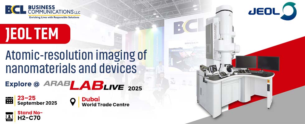
Unlock Atomic Insights with JEOL TEM at ArabLab 2025
Every year, the ArabLab Exhibition brings together scientists, researchers, and innovators from around the world. In 2025, we are once again proud to participate in this global platform. From 23 to 25 September 2025 at the Dubai World Trade Centre, we will showcase advanced laboratory technologies, including the JEOL Transmission Electron Microscope (TEM), a system that is reshaping the way researchers study the microscopic world.
Seeing Beyond the Limits of Light
Modern research depends on the ability to study matter at the smallest scale. Traditional light microscopes have their limitations because they rely on visible light. The electron microscope goes much further by using electron beams to reveal structures at the atomic and molecular level.
The JEOL TEM is one of the most advanced electromagnetic microscopes available. It provides resolution that exceeds the capability of light-based instruments, making it vital for fields such as nanotechnology, life sciences, materials science, and medicine.
JEOL’s Legacy of Precision
JEOL was founded in 1949 and soon after introduced the world’s first Transmission Electron Microscope (TEM). Since then, the company has remained at the forefront of innovation in microscopy.
In the 2025 fiscal year, JEOL reported consolidated net sales of approximately 196.7 billion yen (about USD 1.45 billion). Operating profit rose by nearly 29 percent year-on-year, driven by growth in the semiconductor and life science markets. These industries are fuelling demand for high-precision electron microscopes like the TEM.
The strengths of the JEOL TEM include:
- High resolution that makes atomic-scale structures visible
- Analytical capability that goes beyond imaging with elemental and structural analysis
- Versatile applications across biology, semiconductors, alloys, and nanomaterials
- Proven reliability based on JEOL’s global reputation for precision instruments
A Portfolio Designed for Every Research Need
The Transmission Electron Microscope (TEM) market was valued at around USD 0.89 billion in 2024 and is projected to grow at a CAGR of 4.3 percent through 2032. Some reports place the market closer to USD 2.2 billion in 2024 with higher growth forecasts approaching 9.7 percent by 2030. Demand is expanding rapidly across nanotechnology, materials research, and biomedical science.
JEOL remains one of the top three players in the global electron microscopy market, collectively holding about 77 percent of market share along with Hitachi High Technologies and FEI. The company offers a wide portfolio of TEMs suited for different disciplines.
| TEM Type |
Key Applications |
Typical Advantages |
| Cryo TEM |
Structural biology, protein imaging, virus studies |
Preserves samples in near-native state and provides molecular-level clarity |
| Semiconductor TEM |
Electronics, nanodevices, semiconductor R&D |
Identifies defects and thin film interfaces during chip development |
| Magnetic Materials TEM |
Materials science, data storage, spintronics |
Reveals nanoscale structures and magnetic domains |
| 300 kV TEM |
Advanced research in materials and nanotechnology |
Penetrates dense materials for atomic-scale detail |
| 200 kV TEM |
General-purpose research in polymers and alloys |
Balanced resolution, versatility, and cost effectiveness |
| 120 kV TEM |
Biological samples and soft materials |
Gentle imaging for organic and beam-sensitive specimens |
The broader electron microscopy market is expected to exceed USD 10 billion by 2034. Much of this growth is coming from the Asia-Pacific region, where investments in semiconductor manufacturing and research are driving adoption of TEMs in countries such as China, Japan, Korea, Taiwan, and India.
TEM or SEM – Which Microscope is Right for You?
Researchers often compare the Transmission Electron Microscope (TEM) with the Scanning Electron Microscope (SEM). Both are electron microscopes but they differ in purpose and capability.
| Feature |
Transmission Electron Microscope (TEM) |
Scanning Electron Microscope (SEM) |
| Imaging method |
Passes electrons through ultra-thin samples |
Scans electron beams across sample surfaces |
| Resolution |
Reveals atomic-scale internal structures |
Provides detailed 3D surface images |
| Best for |
Internal analysis of materials, nanostructures, cells, and viruses |
Surface morphology, external texture, and inspection |
| Applications |
Nanotechnology, materials science, life sciences, semiconductor R&D |
Forensics, metallurgy, industrial research, quality control |
The JEOL TEM enables researchers to go deeper by exposing internal structures, making it indispensable in both scientific and industrial environments.
Experience Innovation with BCL at ArabLab 2025
The ArabLab Exhibition 2025 provides an opportunity to experience world-class laboratory technologies first-hand. At Stall h3-C70, BCL will present the JEOL TEM alongside other advanced research instruments.
You will be able to:
- Watch live demonstrations of scientific instruments in action
- Discover how the JEOL TEM can support specific research goals
- Learn about solutions for universities, industrial labs, and research centres
- Connect with BCL experts for personalised advice and guidance
Opening New Frontiers in Research
The JEOL Transmission Electron Microscope is more than a high-resolution imaging tool. It represents the future of research across industries that depend on atomic-scale precision. With the global TEM market valued between USD 1 and 2 billion and expanding steadily, and with JEOL achieving strong financial growth, the opportunities for scientific breakthroughs have never been greater.
Experience Innovation At ArabLab 2025
The ArabLab Exhibition 2025 provides an opportunity to experience world-class laboratory technologies first-hand. At Stall H2-C70, we will present the JEOL TEM alongside other advanced research instruments.
You will be able to:
- Watch live demonstrations of scientific instruments in action
- Discover how the JEOL TEM can support specific research goals
- Learn about solutions for universities, industrial labs, and research centres
- Connect with BCL experts for personalised advice and guidance
Event Details
Location: Dubai World Trade Centre
Date: 23–25 September 2025
Stall No: H2-C70
Join us at ArabLab Exhibition 2025 to see how this powerful electron microscope can transform your research.