This site uses cookies to offer you a better browsing experience. By continuing to navigate through this site or by clicking Approve, you consent to the use of cookies on your device as described in our privacy notice.
Park nano-IR Spectroscopy

Park nano-IR Spectroscopy

A Practical Solution for High-Resolution Material Characterization

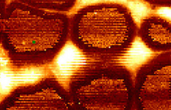
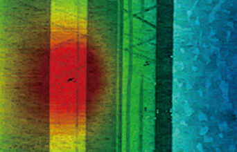
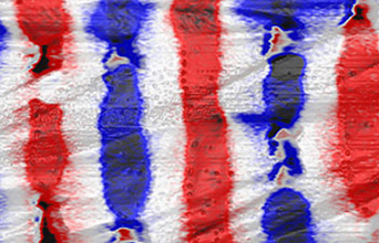
The Park nano-IR system combines nanoscale infrared (IR) spectroscopy with atomic force microscopy (AFM), enabling precise chemical imaging at resolutions beyond conventional methods. With its integration of photo-induced force microscopy (PiFM) technology, the system supports accurate molecular analysis at the nanoscale—down to approximately 10 nm spatial resolution.

Designed to meet the needs of multi-user research facilities, industrial labs, and academic institutions, the system is optimized for ease of use and consistent performance. It is well suited for applications involving sensitive materials and supports a variety of use cases, including chemical mapping, polymer studies, and semiconductor analysis.

Why Choose This System?
Here’s what makes Park nano-IR a smart addition to your lab product line:

  • Easy integration for users already familiar with AFM
  • Perfect for labs needing multi-functional analysis in one tool
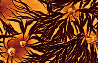
  • Ideal for failure analysis, polymer research, and 2D material studies
  • Saves you time with automated alignment and measurement setup
  • Backed by reliable performance and after-sale support
  • Flexible sizing for sample formats—from small pieces to 300 mm wafers
  • Advanced software with intuitive controls—no extra training needed
Enquiry

Real-World Use Cases

Park nano-IR is commonly used in research and development environments across various domains:

  • Semiconductor failure & defect analysis
  • Biomaterials and soft polymer surface studies
  • Thin film coating development
  • Nanoelectronics and organic semiconductors
  • Photonics, composites & energy materials

Features

Retail-Friendly Feature

  • PiFM-based nanoscale IR imaging
  • Non-contact operation
  • Integrated spectroscopy + mechanical analysis
  • Simple setup with automated probe & beam control
  • Compatibility with AFM software interfaces
  • Built-in multi-mode measurements
  • Scalable (FX200 / FX300 compatible)
  • Cross-comparable with FTIR spectra
  • Pre-sales consultation & post-sales support
  • Compact design, high-throughput performance

End-User Value

  • Clear chemical insights at ~10 nm resolution
  • No tip damage or sample contamination
  • Fewer tools needed—streamlines lab costs
  • Fast onboarding and less downtime
  • No steep learning curve—faster ROI
  • One tool, many experiments—adds value across departments
  • Grows with lab needs—future-ready investment
  • Trusted results aligned with industry standards
  • Reliable service from a retail partner who understands lab needs
  • Saves space, increases productivity

Contact Us at +9714 2152799

We can help you with a solution tailor to your specific need.