Description:
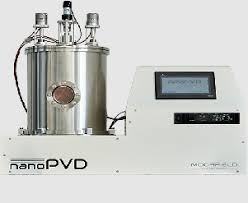
The nanoPVD-S10A is a compact, research-grade benchtop physical vapor deposition (PVD) system optimized for RF and DC magnetron sputtering of both metals and insulating materials such as oxides or nitrides. Designed for substrates up to 4” in diameter, it features up to 3 water-cooled magnetrons for high-power, sustained operation, and a turbomolecular pumping system for ultra-clean deposition environments. Its modular setup supports co-deposition and reactive sputtering using up to three process gases, making it ideal for advanced material development and thin-film research.
Key Features:
- Compact benchtop design
- Up to 3 water-cooled magnetrons for 2" industry-standard targets
- Supports DC and/or RF power sources
- MFC-controlled gas introduction
- Up to 4” substrate compatibility
- Fully automatic operation via touchscreen HMI
- Base pressures <5 × 10⁻⁷ mbar
- Recipe saving and loading for repeatable results
- Cleanroom compatible
- Optional: substrate heating to 500 °C, rotation, Z-shift, shutters, SputterSwitch for source switching
Applications:
The nanoPVD-S10A is ideal for research groups and academic institutions working on advanced material coatings, nanostructured films, and semiconductor device development. It is commonly used for depositing metals, oxides, nitrides, and other compound films for applications in:
- Thin-film electronics: such as sensors, transistors, and photodetectors
- Nano-engineering: creating multilayered structures, barrier layers, and surface treatments
- Optoelectronics & photonics: including reflective coatings, optical filters, and waveguides
- Catalysis & energy research: such as fuel cell electrodes, battery materials, and solar cells
- Dielectric coatings & insulators: for microfabrication and MEMS prototyping
Description:
The nanoPVD-S10A-WA brings wide-area magnetron sputtering to a benchtop format. Built on the nanoPVD-S10A platform, it is designed for uniform deposition over substrates up to 8" in diameter. This configuration uses an upward-facing magnetron source geometry in combination with substrate rotation and orifice exposure plates for enhanced coverage. Like its standard counterpart, it supports reactive and co-deposition processes with high precision and stability.
Key Features:
- Wide-area capability: supports substrates up to 8" diameter
- Benchtop footprint for lab-scale environments
- Water-cooled 2" magnetron sputtering sources
- Touchscreen HMI for full automation and recipe control
- MFC-controlled gas delivery
- Base pressure <5 × 10⁻⁷ mbar
- Optional: 500 °C substrate heating, up to 2 magnetron sources, SputterSwitch technology, co-deposition, pressure control
Applications:
Engineered for larger substrates, the nanoPVD-S10A-WA caters to users requiring uniform thin-film coverage across up to 8” wafers. It’s well-suited for:
- Wide-area device fabrication: including large MEMS structures and display technologies
- Semiconductor wafer processing: for material screening and process development
- Uniform coatings for optics: such as mirrors, anti-reflective layers, and lenses
- Flexible electronics and roll-to-roll R&D: where coverage consistency is critical
- Advanced packaging and multilayer deposition: with co-sputtering and reactive sputtering
Description:
The nanoPVD-T15A is a high-performance benchtop thermal evaporation system for depositing metals and volatile organic materials. Supporting up to 4" diameter substrates, it features a tall chamber for high aspect-ratio coating and can be fitted with both resistive and low thermal mass LTE evaporation sources. Its low base pressure and in-situ process control make it ideal for uniform, contamination-free deposition in research settings.
Key Features:
- Dual-source configuration: for metals and organics
- Up to 4 LTE sources or 2 resistive evaporation sources
- Touchscreen HMI with recipe control
- High aspect-ratio chamber for superior uniformity
- Up to 4" substrate handling
- Base pressures <5 × 10⁻⁷ mbar
- Optional: 500 °C stage heating, substrate rotation, Z-shift, quartz crystal monitoring
Applications:
The nanoPVD-T15A is designed for precision thermal evaporation of metals and organics, making it the go-to system for sensitive or volatile materials. Typical applications include:
- Organic electronics: such as OLED displays, organic solar cells (OPVs), and OTFTs
- High-purity metal films: like gold, silver, aluminum, or chromium for electrical contacts
- Surface coatings in biosensing: for functionalizing surfaces with thin metal layers
- R&D in vacuum coating processes: including mask patterning and lift-off applications
- Materials science and chemical vapor studies: where thermal evaporation yields key insights
Description:
The nanoPVD-ST15A merges magnetron sputtering and thermal evaporation into a single benchtop platform, offering unmatched flexibility for thin-film deposition. Designed for substrates up to 4" in diameter, it accommodates up to three sources of two different types—including LTE, resistive, and magnetron. This versatile tool supports multiple deposition methods in a single run, making it ideal for advanced materials research and multi-layer film development.
Key Features:
- Combines sputtering and evaporation in one system
- Accommodates up to 3 deposition sources (two different types)
- Water-cooled magnetrons for 2" targets
- Touchscreen HMI and recipe control
- MFC-controlled gas delivery
- Base pressure <5 × 10⁻⁷ mbar
- Cleanroom compatible
- Optional: 500 °C heating, substrate motion control, SputterSwitch, co-deposition, quartz sensor monitoring
Applications:
The hybrid nanoPVD-ST15A provides unparalleled flexibility, supporting both sputtering and evaporation workflows in one tool. It’s used across multidisciplinary labs working on:
- Complex multilayer stacks: combining metals, oxides, and organics in a single run
- Prototype device fabrication: such as solar cells, sensors, and photonic structures
- Material development: where comparative studies between deposition techniques are needed
- Quantum and nanoelectronics: requiring ultrathin films with low contamination
- Versatile academic research labs: offering broad teaching and experimental capability in a compact footprint