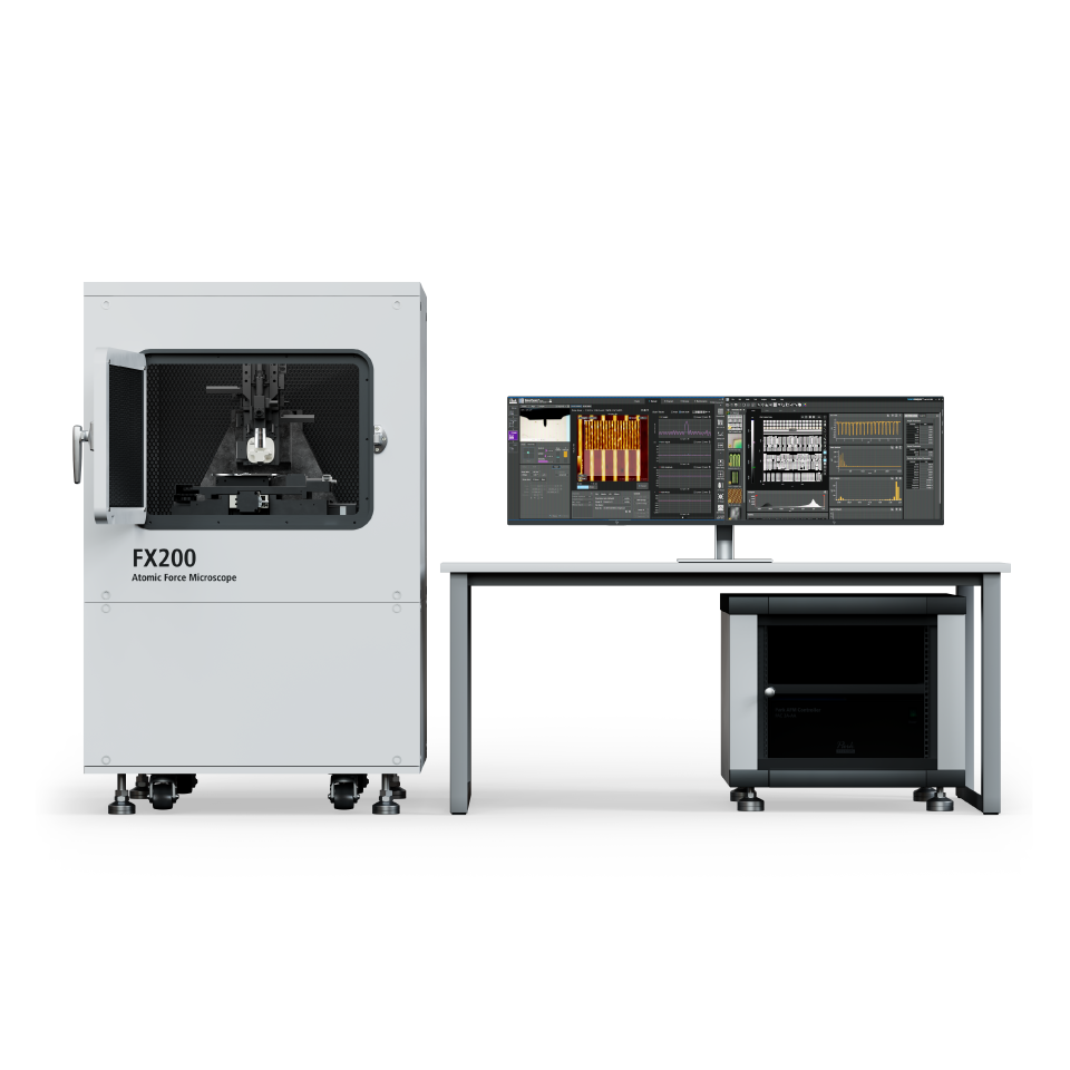
Efficient and reliable products for all your unique requirements.
We offer services that prioritize customer satisfaction at every step.
Experience next-generation nanoscale measurement with Large Sample Atomic Force Microscopes (AFMs)—engineered for high-performance semiconductor metrology and industrial research. Designed to accommodate full wafers up to 300 mm, these systems provide the precision required for complex 3D structures, failure analysis, and device inspection. With Park’s proprietary True Non-Contact™ Mode, they deliver accurate imaging while preserving both tip and sample integrity. Seamlessly integrating into R&D and QC workflows, Large Sample AFMs combine SmartScan™ automation with a user-friendly interface, streamlining operations for consistent, reproducible results. Whether for surface roughness, electrical characterization, or packaging-level metrology, these versatile tools empower teams across semiconductor, materials science, and electronics domains.
EnquiryTake research-grade performance to the next level with the Park FX200, offering high-resolution imaging and full automation for 200 mm wafer samples. With a True Non-Contact™ mode, low thermal drift, and Park’s dual-servo XY scanning, FX200 delivers the perfect blend of control, speed, and repeatability.
Smart automation handles laser alignment, probe exchange, and image optimization. Meanwhile, the intuitive software and robust hardware make it easy for any lab to generate highly reproducible results with confidence.
Why FX200?
Engineered for advanced semiconductor processing, the Park FX300 handles 300 mm wafers with ease. Whether for failure analysis, electrical characterization, or process validation, FX300 empowers your team with next-gen automation and exceptional measurement precision.
Industrial-grade safety features, optional fan-filter unit (FFU), and fast Z servo performance make this system a powerhouse for inspection, metrology, and real-time control in cleanroom or production environments.
Why FX300?
The Park NX20 is the ultimate platform for defect imaging, surface roughness measurement, and semiconductor failure analysis. Equipped with True Non-Contact™ mode and a decoupled XY scanning system, it delivers sharp data with minimal tip wear—even at high speed.
SmartScan™ software and step-scan automation help engineers capture defects fast and reproducibly. With electrical, magnetic, and topographic mode support, the NX20 offers unmatched value for labs tackling detailed investigations.
Why NX20?
When wafer-level inspection requires uncompromising accuracy, choose Park NX20 300mm. Built on the NX20 platform with a 300 mm motorized stage, it supports advanced automation and full-device inspection in one seamless workflow.
From electrical failures to roughness measurements, this system supports comprehensive AFM modes tailored for QC and FA engineers working with large samples—without the need to move or reposition wafers.
Why NX20 300mm?
The Park NX15 is the most affordable, research-ready AFM for large samples. Ideal for shared labs and budget-conscious teams, it delivers powerful imaging, smart automation, and advanced electrical measurement capabilities—all in one compact, flexible unit.
With support for multi-sample imaging, accurate XY scanning, and True Non-Contact™ mode, NX15 maximizes throughput and delivers exceptional data—without sacrificing cost-effectiveness.
Why NX15?
Large Sample AFM Series Experience the tangible advantages of Park’s Large Sample AFMs—maximizing performance, minimizing effort, and accelerating your nanoscale success.
Explore advanced engineering and intelligent automation built into every Large Sample AFM—designed to deliver exceptional precision at scale.
We can help you with a solution tailor to your specific need.